 Polski
 English
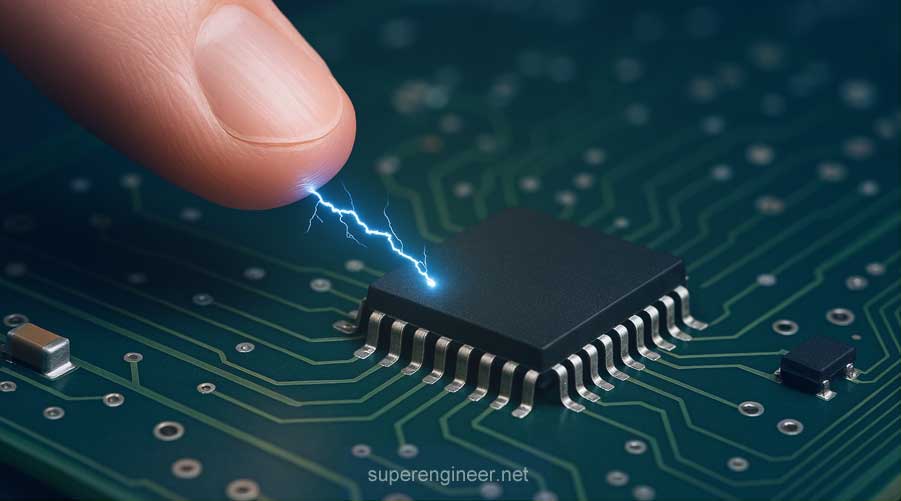
Introduction
Electrostatic Discharge (ESD) is a physical phenomenon that poses a serious problem in certain industrial sectors. ESD is particularly troublesome in the semiconductor industry, electronic device assembly, printing, flammable materials, and anywhere a small electric arc can "ignite" something…
The ESD phenomenon is closely related to the properties of materials (insulators that easily become charged) and to air humidity (the lower the humidity, the greater the ESD risk). Managing this problem requires appropriate efforts in the following areas:
- Product design with regard to ESD protection.
- Manufacturing processes, where ESD events can occur at various production steps.
This article discusses the ESD phenomenon with particular focus on its impact on electronics, though the information presented will also be useful for other industries.
Enjoy the read :)
ESD Phenomenon
ESD is a physical phenomenon involving the rapid flow of static electric charge between two objects with different electrostatic potentials. It typically occurs when a charged object comes close to another object, resulting in a small electric spark between them.
A common everyday example is the noticeable "electric shock" when touching a doorknob after walking on a carpet. That "shock" is the electrostatic discharge in the form of a spark.
In industrial environments, objects such as moving conveyor belts, packaging films, workers' clothing, or the product itself (e.g., a printed circuit board being transported on an assembly line) can become electrostatically charged.
According to industry experts, ESD is defined as the "sudden, spontaneous flow of electrostatic charge caused by a high electrostatic field".[1]
Electrostatic charge accumulates on a surface due to the following phenomena:
Triboelectric Effect
The most common phenomenon. Triboelectric charging, also known as the triboelectric effect, is the generation of electrostatic charge on the surface of a material when two materials come into contact and are then separated. During this process, one material gains excess electrons while the other loses them. As a result, the first material becomes negatively charged, and the second positively charged. Typical examples include:
- Sliding a PCB across a tabletop.
- Walking on a carpet.
- Inserting a PCB into a plastic device enclosure.
- Peeling off protective film from a device casing.
- Friction between materials, clothing, packaging, etc.
Induction
In the context of ESD, induction is a phenomenon in which electrostatic charge appears in a conductor without direct physical contact with a charged object, but as a result of the influence of its electrostatic field.
For example, when a highly charged object approaches an ungrounded conductor (e.g., a metal tool), the electric field of the charged object affects the free electrons in the conductor. These electrons are displaced, causing a local accumulation of charge. If the charged conductor is then touched, an ESD event may occur.
Ion Bombardment
Sounds like a scene from a science fiction movie :) Ion bombardment is the phenomenon of gradual charging of a material due to the accumulation of ions (charged particles) on its surface, which transfer their charge. This can occur, for example, during coating processes or semiconductor manufacturing.[2]
ESD Effects
ESD events can occur on a very small scale — below the threshold that causes damage. They can also reach levels that cause equipment malfunction without permanent damage. In some cases, the discharge can be strong enough to physically damage the equipment. In certain industries, ESD can also pose a safety risk to personnel or infrastructure.
Depending on the energy of the discharge, several types of ESD effects can be distinguished:
- Immediate damage. These are permanent failures that result in the immediate loss of functionality of a component or device. If they occur during the production process, they are typically detected during production testing.
- Latent defects. These are particularly problematic types of damage. A component may initially function correctly with minor parameter deviations, but over time the damage worsens, potentially leading to unpredictable failure during the device's operational life.
- Soft ESD. ESD events can cause disruptions in digital circuitry. They may manifest as software freezes or incorrect logical behavior. A small ESD event can trigger a "latch-up," causing logic gates to lock up. These disruptions often disappear after a power reset and do not cause permanent hardware damage.
- Safety hazards. In industries such as chemical, petrochemical, or pharmaceutical, ESD can pose a direct safety threat. Electrostatic discharges can ignite gases, dust, fuel vapors, or even detonate explosive materials. In such environments, proper ESD control is critical to preventing serious accidents.
- Other effects. ESD phenomena can also interfere with technological processes — for example, causing paper to stick together, attracting dust to sheet surfaces in printing plants, or disrupting the operation of machine controllers or other industrial automation systems.
ESD Models
ESD phenomena occurring during the electronics assembly process and during device operation have been described using specific models. These models allow for testing the immunity of products or test components sensitivity to ESD, referred to as ESDS (Electrostatic Discharge Sensitive). The following models have been developed:
- HBM (Human Body Model). This model simulates a charged conductor (including a person) discharging electrostatic charge into an ESDS component. It is the most commonly used model for testing the ESD immunity of integrated circuits and reflects typical situations in electronics assembly.
- CDM (Charged Device Model). CDM simulates a situation where a charged ESDS component touches a conductive object. For example, during automated assembly, a component moves through an insulated feeder, accumulates charge, and then rapidly discharges upon contact with a grounded machine element.
- MM (Machine Model). The MM model simulates a situation where a component contacts a charged machine or tool. It is based on a 200 pF capacitor without a current-limiting resistor. Due to its limited practical relevance, it is now rarely used and has been largely replaced by HBM and CDM.
- IEC 61000-4-2. The model defined in the IEC 61000-4-2 standard represents ESD events that may occur during device operation in real-world environments, such as when a user touches a USB port. This model is used for testing the immunity of the entire system (end product).
ESD & Product Design
ESD immunity shall be addressed at the electronics design stage. It is essential to meet the requirements related to electrostatic discharge immunity during device operation (e.g., IEC 61000-4-2, EN 55024, ISO 10605, etc.). Typical aspects to consider include:
- System-level I/O protection. Use of protection devices such as TVS diodes, clamping diodes, or small capacitors on the inputs/outputs of external interfaces (USB, HDMI, Ethernet, antenna connectors, GPIO ports, etc.). These components should be placed as close to the connector as possible.
- Proper PCB layout. The impact of ESD on electronics can be significantly reduced by following design recommendations for trace routing and component placement on the PCB. This includes minimizing ground path impedance, separating sensitive circuits, shielding, using ESD grounds, and routing traces away from edges or enclosure walls.
- Component selection. Certain components, such as I/O interfaces, CAN, RS485, etc., should be selected with ESD immunity in mind. It is important to distinguish between HBM and CDM models, which relate to the robustness of individual components, and the IEC 61000-4-2 model, which represents ESD events in real-world usage conditions.
- Shielding. Using metal shields and conductive layers on enclosures or shielded cables is effective in reducing both electromagnetic interference (EMI) and the effects of electrostatic discharges (ESD). The shield/enclosure design should enable fast and controlled dissipation of electrostatic charge to a reference potential (ground).
ESD & Manufacturing Process
Effective protection against ESD in the electronics assembly process requires the implementation of an ESD control program, in accordance with ANSI/ESD S20.20 (or IEC 61340-5-1). This system shall include collective protection measures (e.g., flooring), personal protection (e.g. footwear), monitoring (periodic ESD measurements), and personnel training. Key aspects include:
- Grounding of work surfaces. Workbench tops, carts, racks, and all contact surfaces should be made of ESD-safe materials and connected to a grounding point via a resistor. The surface voltage should not exceed specified limits (typically ±100V relative to ground).
- Personal ESD protection equipment. Typical solutions include wrist straps and ESD footwear. Both should be tested before entering the EPA (Electrostatic Protected Area).
- Use of ESD-safe containers and bags. Every ESDS (Electrostatic Discharge Sensitive) component should be stored and transported in protective packaging. Regular plastic trays, common plastic bags, and styrofoam are not allowed.
- Monitoring. Periodic testing of surface resistance and grounding resistance should be performed. Footwear and wrist straps should be tested. Materials, packaging, and tools used in the process shall be verified. Records of these measurements shall be maintained.
- Personnel training. All employees handling ESDS components—regardless of role (operators, technicians, engineers, warehouse staff) shall undergo ESD training. Training shall be documented and periodically refreshed (e.g., every 12 months).
A complete ESD protection program includes numerous requirements. For instance, ambient humidity shall be monitored and controlled, and ionizers may be required in specific parts of the process.
ESD Standards in Electronics
- ANSI/ESD S20.20. A core standard developed by the ESD Association (approved as an ANSI standard), describing the principles of an organizational ESD control program. It defines requirements for EPA zones, grounding, protective clothing, personnel training, audits, and more.
- IEC 61340-5-1. An international standard (IEC) focused on protection against static electricity. Its content is similar to ANSI/ESD S20.20. In many countries, it is adopted as a national standard.
- IPC-A-610. A standard covering the acceptability of assembled electronic products. It also includes guidelines for handling electronic assemblies and emphasizes the importance of ESD protection during inspection and handling.
- IPC J-STD-001. A joint IPC/JEDEC standard for soldering and assembly processes. It includes requirements for maintaining ESD-safe practices during manufacturing and handling of sensitive components.
- JEDEC JESD625-A. A JEDEC standard that specifies handling requirements for electrostatic discharge sensitive devices (ESDS). It primarily applies to semiconductor manufacturers and component distributors.
- IEC 61000-4-2. A system-level EMC standard specifying test methods for the immunity of electronic equipment to electrostatic discharges during use (product-level ESD testing).
- JEDEC/ESDA JS-001 and JS-002. Joint standards by JEDEC and the ESD Association defining HBM (JS-001) and CDM (JS-002) test methods. These replace older standards JESD22-A114 and JESD22-C101. Semiconductor manufacturers use these documents to classify ESD immunity levels (e.g., HBM Class 2 - 2kV).
- ISO 10605. An automotive ESD test standard for vehicles and vehicle components. It is quite similar to the IEC 61000-4-2, but tailored for the automotive environment, with different voltage levels and test setups for both human interaction and charged components.
The standards listed above are only selected examples — many additional guidelines exist, including the ANSI/ESD S1-S20 series, advisory documents (e.g., ESD TR20.20), and industry-specific standards applicable in other sectors.
Summary
Effective protection of electronic devices against ESD requires a comprehensive approach. ESD-related risks should be considered as early as the design stage — this includes selecting appropriate components, distinguishing between HBM/CDM and IEC models, designing the PCB correctly, and implementing proper input/output protection. During manufacturing, compliance with ANSI/ESD S20.20 or IEC 61340-5-1 is essential to minimize the risk of damage.
In short: "It takes two to tango" — effective ESD protection requires both a well-designed device and a properly controlled production process.
References
- https://www.esda.org/
- H. Ichikawa, M. Ito, K. Hamada, A. Yamaguchi, and T. Nakabayashi, "Electrostatic-discharge-induced degradation caused by argon ion bombardment in facet-coating process of GaInAsP/InP laser diode," Japanese Journal of Applied Physics, vol. 47, pp. 7886–7889, 2008, doi: 10.1143/JJAP.47.7886.
