 Polski
 English
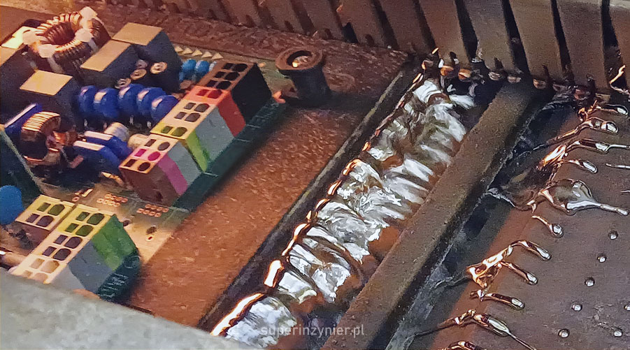
Introduction
The wave soldering process can only be carried out with the required level of quality if certain technical requirements are met. It is necessary to supply the right quality materials: components with the correct solderability, adequate soldering flux and the correct lead-free alloy or lead based alloy.
In addition to the materials themselves, a very important aspect is the correct time-temperature profile of wave soldering process, which is the subject of this article.
It is worth knowing that reflow soldering is another process in which the right SMT solder paste and the correct SMT profile are key aspects of quality solder connections.
An incorrectly set soldering profile may lead in some cases to phenomena such as nonwetting or dewetting.
Wave soldering
Before discussing the temperature-time profile requirements, it is necessary to say a few words about the wave soldering process itself. It takes place in a soldering machine called a " soldering aggregate" or colloquially "the wave". We can distinguish the following steps of the process:
- Loading. The proper direction of the PCB board in the soldering process is a crucial aspect. Depending on the PCB project, this can have a significant impact on the soldering quality.
- Fluxing. A flux is applied to the entire bottom surface of the circuit board. There are various methods of flux application, usually using spray, sometimes foam (foam fluxing) or spraying with a drum (drum spraying). Less common methods include "microjet" or dipping.
- Preheating. This stage involves gradually raising the temperature of the PCB to the level required by the flux spec. The soldering machine can have one or more heating zones. Various methods are used: infrared lamps (short-wave infrared), calrod heaters (medium- and long-wave infrared) or convection heaters (hot air).
- Contact with solder. At this stage, the heated PCB comes into contact with the melted, "wavy" solder. This can be compared to the fact that the PCB is like a "surfer on a wave". There are several technical solutions related to shaping the appropriate waveform of liquid solder. The solder unit can be equipped with a single or double wave, called turbulent (Chip wave) and laminar (Main wave). There is also a Worthmann wave, which resembles a combination of a turbulent wave and a main wave. When soldering, an additional nitrogen shield is often used to improve soldering quality and reduce tin dross.
- Cooling. After the PCB board leaves the "wave area", it enters the cooling area, where forced convection is used to cool down the board.
Wave soldering profile
The temperature-time profile begins shortly after applying flux, when the PCB is introduced into the heating zone. The following stages can be distinguished:
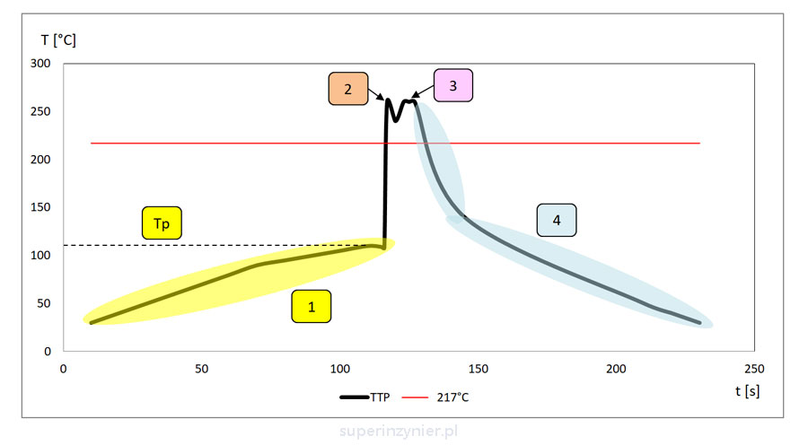
- Preheating [1]. It is the gradual raising of the temperature of the PCB to a level in the range of 70-130C, typically 90-110C. The specific temperature value Tp depends on the requirements of the flux and the limitations of the components used. The PCB surface temperature should be measured according to flux recommendations, typically on the solder destination side of PCB, that is, "on top of the board". During preheating, the maximum temperature gradient for components of 3C/s[1] should not be exceeded. The purpose of the preheating step is:
- Solvent evaporation. Alcohol or water serves as a "solvent" (so called the carrier), which needs to be removed before coming into contact with liquid solder. This significantly reduces the amount of tin balls.
- Flux activation. Weak organic acids in the flux activate at a specific temperature, removing metal oxides (tin oxides) from solder pads and component leads.
- Reduction of thermal stress on components. Heating components before they come into contact with liquid solder reduces the temperature difference, thus minimizing the thermal shock to which components are subjected.
- Chip Wave [2]. If a soldering machine has a chip wave activated, then it appears in the soldering profile as the "first peak". The chip wave is very turbulent in order to reach small SMD solder lands, even when those lands are sometimes "shadowed" by other components.
- Main Wave [3]. The PCB board is moved over agitated, molten solder called the "main wave". The alloy covers solder pads and component leads for a specified time, typically 2-4 seconds. The molten solder is heated to a specific temperature. For SAC lead-free alloys, the range is 260-270C, while for lead-based alloys, this temperature is lower, around 240-250C.
- Cooling [4]. After the board exits the soldering "wave" area, cooling occurs, typically using fans. The temperature gradient should not exceed 6°C/s[1].
Copper dissolution
During the soldering process, component leads and PCBs come into contact with molten solder and then a small amount of copper dissolves into the molten alloy. This is a phenomenon called copper dissolution. In this context, it is crucial to control the contact time and temperature of the alloy, as these factors significantly affect the amount of copper dissolved.
Summary
Wave soldering requires ensuring an appropriate temperature-time profile. As a starting point, it is necessary to consider the flux requirements, i.e., the temperature of the PCB surface on the solder destination side, before the board contacts the liquid solder. In addition, it is necessary to ensure compliance with component requirements, i.e., not exceeding the maximum heating gradient. Some components, such as film capacitors, are very sensitive to temperature, and their soldering requires a special attention. Solder contact time should be selected through experimentation, minimizing stress on components.
The amount of flux should be selected to ensure correct soldering and, at the same time, not so much as to keep the level of ionic contamination low, which has a significant impact on the reliability of the soldered device.
If special solder carriers (pallets) are used in the wave soldering process, covering part of the PCB, it may be difficult to heat the PCB evenly. This creates the risk of greater contamination with flux residues. In such cases, the correct design of the soldering frame, the correct application of flux, and the optimal method of heating the PCB are crucial for the quality of solder joints.
Przypisy
- IPC/JEDEC J-STD-020
