

What is a Via?
A via is a small, copper-plated hole in a PCB that acts as an interconnection between copper tracks at various layers. These vias allow electrical signals or power to flow through the tracks.
The IPC-T-50 standard defines a via as: "A plated hole that is used as an interlayer connection but is not intended for inserting a component lead or metallic part."[1]
Vias are classified according to their structure and connection to different PCB layers. These categories include through-hole via (1), blind via (2), buried via (3), microvia (4) and back-drilled via (5).
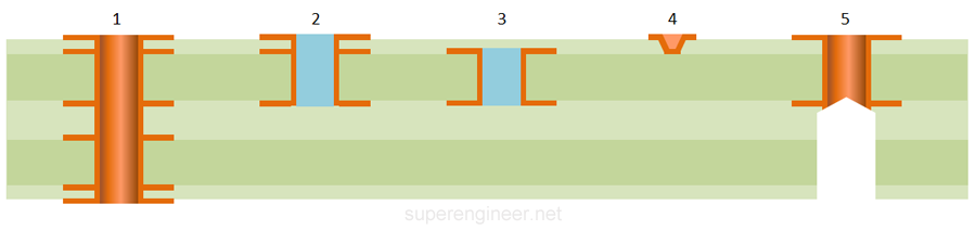
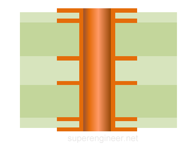
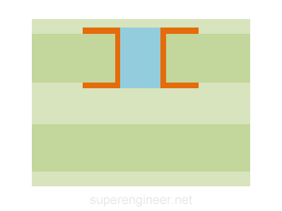
Through-hole via
A through-hole via extends through the entire thickness of the PCB. It is visible from both the top and bottom surfaces of the PCB board.
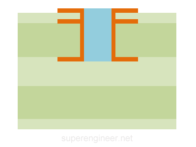
Blind Via
A blind via connects tracks at external layer to one or more tracks located in internal layers, without going through the entire board. This type of via is not visible from the opposite side of the PCB.
There are several methods for creating blind vias:
- Sequential lamination. This process involves laminating multiple thin double-layer cores that were previously etched and plated. It is costly and thus rarely used.
- Photo-defined. This method uses a photosensitive resin layer applied to the core. After exposure, curing, and etching, areas down to the core traces are exposed. Plating then provides the electrical connection. This process can be performed simultaneously on both sides of the core, enabling the rapid production of a large number of vias.
- Controlled-depth drilling. A non-through (blind) hole is drilled from the external layer to one or more internal layers. The hole is then plated to ensure proper electrical connection.
- Laser drilling. A non-through (blind) hole is created using a laser, followed by plating to establish the electrical connection.
Buried Via
A buried via connects copper traces only between internal layers. The structure of this via is not visible from either external surface of the PCB.
Microvia
A microvia is significantly smaller than a traditional via and is used to connect two adjacent layers. The hole is created using a laser and then plated.
IPC-T-50 defines a microvia as a blind via with a maximum aspect ratio of 1:1 and a maximum height of 0.25 mm.[1]

Microvias can be arranged in a staggered (1) configuration or stacked (2) directly on top of each other, as shown in the illustration below:

Backdrilled Via
A backdrilled via is a standard through via where the unnecessary copper section, known as the "stub," is removed through precision backdrilling with controlled depth.
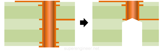
This type of via is used in high-frequency signal circuits to improve signal integrity.
Via Protection Methods
Copper plating in vias requires additional protection to minimize the risk of corrosion. Several protection methods are used:
- Standard finish. The copper surface of the via is covered with the same finish as the solder pads. Common finishes include ENIG, HASL, immersion tin, OSP, and others.
- Tenting. The via hole is covered with a solder mask, applied as either a dry film or a wet film.
- Plugging. The via hole is filled with a dielectric material and optionally covered with a solder mask.
- Filling. The via hole is completely filled with epoxy or conductive material. The surface may be fully plated with copper and, in some cases, covered with a solder mask.
The Global Electronics Association (IPC) organization has developed the IPC-4761 standard, which classifies vias into types 1 through 7 based on the protection method used.
Advantages of Vias
- Vias provide electrical connections between copper traces on different PCB layers, enabling board miniaturization.
- Vias can serve as thermal paths, improving heat transfer from power devices through the laminate to a heatsink.
- Vias can assist with circuit shielding, such as forming shielding vias densely arranged to block certain electromagnetic waves.
Disadvantages of Vias
- Vias may crack due to differences in the coefficient of thermal expansion (CTE) between the laminate and the via plating. Careful material selection, via dimensions, and plating thickness are essential to minimize this risk.
- Vias can fail due to electrochemical migration or plating corrosion caused by contaminants such as PCB processing chemicals, flux residues after soldering, moisture, and more. Reducing this risk involves protecting the via plating through appropriate finishes, masking, or filling.
- Vias affect signal integrity. Therefore, their number should be minimized in high-frequency circuits, often replaced with buried, blind, or backdrilled vias instead of standard through vias.
- Vias can reduce the effectiveness of ESD / EOS protection in circuits with TVS if they are poorly positioned on the PCB.
Summary
The best type of via is no via at all, which is why we strive to reduce their number wherever possible, especially in circuits where vias degrade signal integrity.
There are also cases where additional vias are needed to lower impedance between layers or improve heat transfer. Vias can also be added to ensure connection redundancy in case of failure.
If a via is necessary, it is essential to consider DFM (Design for Manufacturing) and DFR (Design for Reliability) principles. Choosing the right type of via depends on many factors. Quality, reliability, and miniaturization requirements often conflict with manufacturing costs, requiring careful design decisions.
To improve reliability, vias are protected using methods such as standard finishes (HASL, ENIG, etc.), solder mask tenting, plugging, or filling. Detailed information can be found in the IPC-4761 standard.[2]
The reliability of vias depends on selecting the appropriate type for a given application and operating conditions. Geometry (e.g., plating thickness) and protection methods also play a critical role. Using the proper via type and protection can minimize the risks of cracking, corrosion, and signal integrity issues.
References
- IPC-T-50: Terms and Definitions for Interconnecting and Packaging Electronic Circuits, Rev. N, IPC International, USA, 2021.
- IPC-4761: Design Guide for Protection of Printed Board Via Structures, IPC International, USA, 2006.
