
 Polski
 English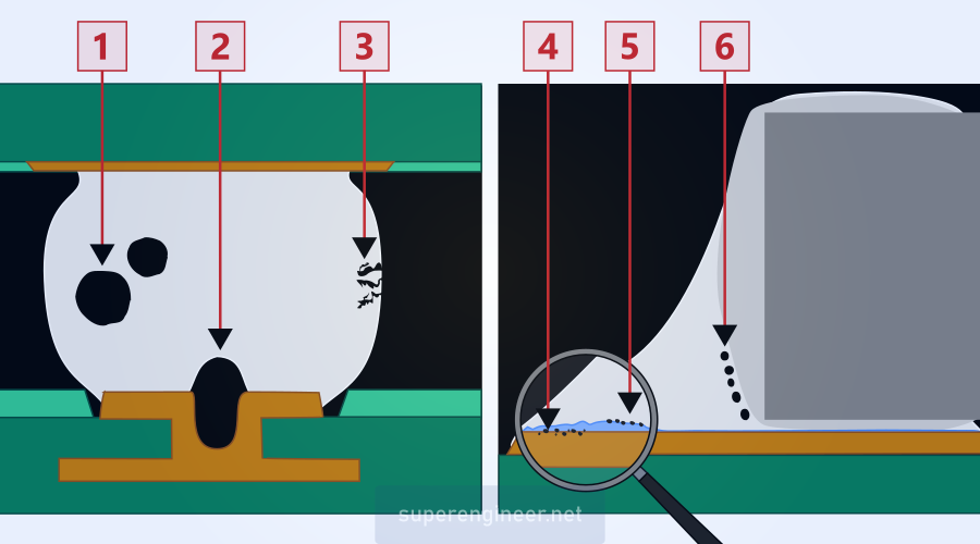
Introduction
Voids in solder joints are a phenomenon that has been present in the electronics industry since its very beginning. Certain types of voids occur frequently and are considered acceptable in many applications. However, there are also voids whose presence is undesirable, as they can degrade solder joint reliability. Much depends on the void type, their location, and of course the end-use application of the electronic device. Some industries within the ADHP (Aerospace, Defense, High Performance) group place great importance on voiding in solder and actively strive for significant void reduction.
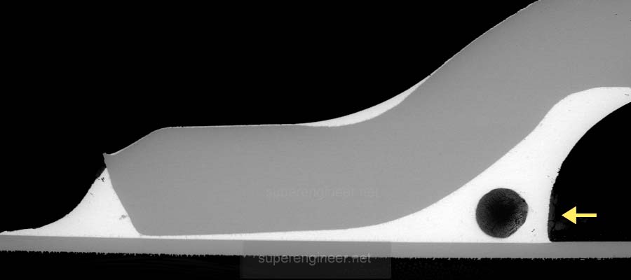
An example of a process void (large) visible in a cross-section through a solder joint. SEM image:
and example voids visible in the X-ray image of BGA solder joints:
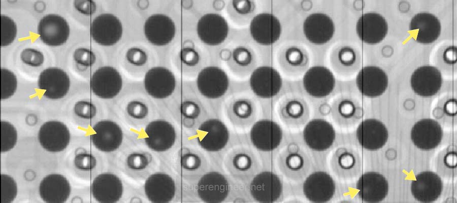
This article covers the types of voids in solder joints, their causes, and the requirements of the major IPC standards on this topic. Read on.
Process Voids
Process voids are typically oval, randomly distributed voids within the solder bulk, usually located closer to the central part of the joint. These voids are detectable by standard X-ray inspection. Typical diameters range from 50 to 300µm, classified as macrovoids, while voids smaller than 50µm are classified as microvoids.
Causes: Process voids are associated with the soldering process or moisture in the materials. They form when volatile flux decomposition products fail to escape from the solidifying solder before it freezes. A second source of voids is moisture trapped in the solder paste or the PCB laminate itself, which outgasses during the soldering process.
Solutions: Optimization of the SMT reflow profile (extended soak zone to drive off flux volatiles, appropriately set TAL). Use of low-voiding SMT solder paste. Reflow soldering in a vacuum or reduced-pressure oven. Use of nitrogen (N2) atmosphere. Appropriate stencil aperture design (e.g., segmentation of large pads), among others.
Acceptance Criteria: IPC standards such as IPC J-STD-001, IPC-A-610, and IPC-7095 define the maximum void limit for BGA solder joints (collapsing solder balls) as maximum 30% of the X-ray ball image area[1,2,3]. Requirements are also established for the thermal pad of BTC (e.g., QFN) joints, where voids up to 50% of the pad area are considered an acceptable condition per IPC, for all product classes[2,3].
Via-in-Pad Voids
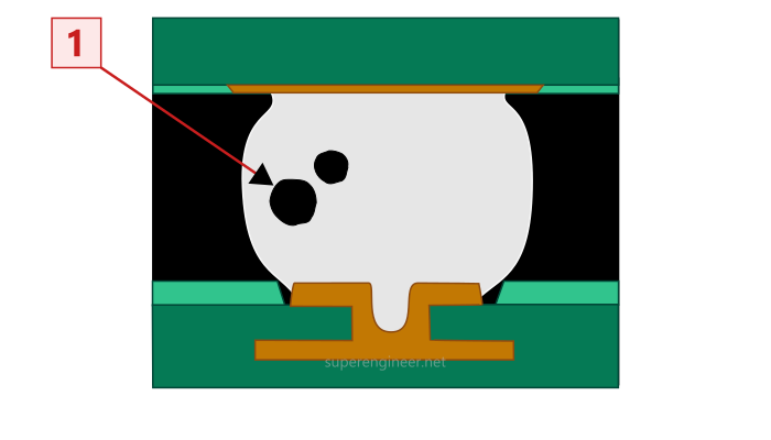
Via-in-pad voids can occur when microvias are located within the solder pad — a configuration known as via-in-pad. In such cases, the void forms directly above the via. This situation is most commonly encountered in BGA assembly, where a microvia is connected to the SMT pad of a given device.
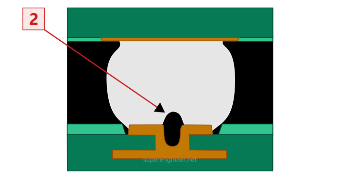
Causes: In PCB designs utilizing microvias in pads, voids can form as a result of outgassing from flux, moisture, and air trapped within the microvia itself.
Solutions: Avoid microvias in pads where possible, or use vias that are filled and capped with copper (Type VII per IPC-4761).
Acceptance Criteria: Voids caused by the via are classified as "design-induced." In such cases, IPC-A-610 does not define acceptance limits, leaving this matter to be agreed upon between the customer and the supplier (user and manufacturer)[3].
Shrinkage Voids
Shrinkage voids are irregular surface depressions that penetrate into the solder bulk, often with an irregular shape. This phenomenon is generally considered to have no impact on solder joint quality or reliability.

Causes: Non-uniform shrinkage of lead-free alloy during solidification. The phenomenon is related to the alloy type, i.e., its chemical composition. Another important factor is the solidification rate, which depends on the solder volume, pad size, and process parameters — particularly the cooling rate.
Solutions: The phenomenon is cosmetic in nature and is not considered a defect in the industry. Minimization can be achieved by substituting a non-eutectic lead-free alloy (e.g., SAC305) with one closer to eutectic composition (e.g., SAC387). Modifying pad geometry or reducing the PCB cooling rate during the soldering process may also be beneficial.
Acceptance Criteria: IPC-A-610 classifies this phenomenon as an acceptable condition for all IPC product classes — Class 1, 2, and 3[3].
IMC Micro-Voids
Sub-micron voids in the intermetallic compound (IMC) layer — referred to as IMC micro-voids — are microscopic voids that form within or at the boundary of the IMC layer. Two distinct situations with different origins are recognized. The first are Kirkendall voids — submicron voids located at the Cu/Cu3Sn interface and within the Cu3Sn layer itself[5]. The second are voids in the IMC region whose origin is not the Kirkendall effect, but rather inclusions (organic contaminants) introduced into the copper during the electroplating process[4].

Causes: The first cause is the Kirkendall Effect (diffusion mechanism): the formation of intermetallic phases between dissimilar metals (copper and tin) involves atomic diffusion proceeding at different rates. Copper atoms migrate faster than tin atoms, leading to the formation of submicron voids on the copper side — at the Cu/Cu3Sn interface and within the Cu3Sn layer. This effect is intensified by elevated operating or storage temperatures, which accelerate diffusion. If the number of these voids increases significantly, it may adversely affect solder joint reliability under mechanical loading conditions (e.g., mechanical shock, drop test)[1]. A second, diffusion-independent source of micro-voids in the IMC region is organic contamination entrapped in the copper during electroplating[4].
Solutions: For diffusion-induced voids (Kirkendall): doping the solder alloy with additional elements (e.g., Zn and others)[1,5] and the use of a nickel diffusion barrier, i.e., selecting boards with PCB pad finishes such as ENIG. For contamination-induced voids: ensuring a clean and stable copper electroplating process at the PCB supplier (high-purity Cu, organic contamination control).
Acceptance Criteria: IPC acceptance standards (IPC-A-610, J-STD-001) do not define limits for this type of micro-void.
Pinhole Micro-Voids
Micron-scale voids located within the intermetallic layer, at the interface between the IMC and the copper pad, or near the IMC layer on the solder side[4].

Causes: An unstable electroplating process at the PCB manufacturer. Defects and contaminants introduced into the copper pad coating during metallization manifest during soldering, when the molten alloy reacts with copper to form the intermetallic layer. Local coating defects then remain as micro-voids within or at the boundary of the IMC[4].
Solutions: Ensuring a stable, controlled electroplating process and high pad cleanliness at the PCB supplier.
Acceptance Criteria: IPC acceptance standards (IPC-A-610, J-STD-001) do not define limits for this type of micro-void.
Planar Micro-Voids
Planar micro-voids (also known as champagne voids) are clusters of very fine bubbles (<20µm)[4] lying in a single plane at the solder-PCB pad interface or the solder-component lead interface. Their resemblance to champagne bubbles gives rise to the widely used alternative name "champagne voids." When these voids occur in large numbers within a given plane, they can adversely affect solder joint reliability. These fine voids are not detectable by standard 2D X-ray analysis due to the limited resolution of the equipment.
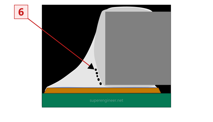
Causes: The phenomenon is most commonly associated with anomalies in surface finishing processes: metallization and electroplating of component leads and PCB pads. In the past, immersion silver (IAg) PCB pad finish was suspected of promoting this type of voiding; however, today, with appropriate process chemistry, this risk has been significantly reduced[1].
Solutions: Optimization of component lead and PCB pad surface finish processes. Ensuring high cleanliness of component leads and PCB pads.
Acceptance Criteria: Industry standards such as IPC-A-610 and J-STD-001 do not define acceptance limits for this type of void.
Summary
Voids in solder joints are an unwanted phenomenon inherent to the soldering process. Some void types, such as process voids (macrovoids), are broadly acceptable in consumer applications and many professional use cases. In high-reliability applications, however, certain process voids may be viewed as a reliability risk.
Oddly enough, the voids that can pose a real threat to solder joint reliability are not the large, process-related bubbles easily visible in X-ray imaging, but rather the fine micro-voids near component leads - or right at the interface and within the intermetallic layer. In high-reliability applications, every effort should therefore be made to minimize the risk of this type of voiding. Material selection plays a primary role here: solder alloy, PCB pad finishes, and component lead finishes. The second important aspect is proper process control, as well as monitoring solder joint quality through metallographic cross-section analysis using scanning electron microscopy (SEM).
References
- IPC-7095 Rev.E, Design and Assembly Process Implementation for BGAs, IPC International Inc. USA, 2022.
- IPC J-STD-001 Rev.J, Requirements for Soldered Electrical and Electronic Assemblies, IPC International Inc. USA, 2024
- IPC-A-610 Rev.J, Acceptability of Electronic Assemblies, IPC International Inc. USA, 2024
- IEC TR 61191-8:2021, Printed Board Assemblies - Part 8: Voiding in Solder Joints of Printed Board Assemblies for Use in Automotive Electronic Control Units - Best Practices, 2021
- J. Yu and J. Y. Kim, "Effects of residual S on Kirkendall void formation at Cu/Sn-3.5Ag solder joints," Acta Mater., vol. 56, no. 19, pp. 5514-5523, 2008
